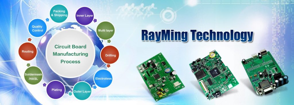
A printed circuit board (the PCB abbreviation of the expression “Printed Circuit Board” is also used) is a support, generally a plate, for electrically connecting a set of electronic components to each other, in order to make a circuit complex electronics. It is also referred to as the electronic card.
It consists of an assembly of one or more thin layers of copper separated by an insulating material. The copper layers are etched by a chemical process to obtain a set of tracks, terminated by pellets. The printed circuit is often covered with a layer of colored varnish that protects the tracks from oxidation and possible short circuits.
The tracks electrically connect different areas of the printed circuit. The pellets, once perforated, establish an electrical connection, either between the components welded through the printed circuit, or between the different layers of copper. In some cases, non-perforated pellets are used to weld surface-mounted components.
Printed Circuit Board Development:
There are many different types of circuit board assembly used in industrial manufacturing of electronics. With the decrease in manufacturing costs, the number of layers used by printed circuits for consumer applications continues to increase. While in the 1990s, the automotive industry considered that only single-sided PCBs were industrially acceptable, it is no longer surprising to encounter four-layer circuits in consumer devices, and from 10 to 14 layers for specific applications. Generally, we alternate layers carrying the signals and more homogeneous layers (ground plane and power plane) in order to distribute the supply voltages on the whole map and improve the electromagnetic compatibility (abbreviated as CEM). The different layers are interconnected by metallized holes called vias. Recent techniques make it possible to make blind vias (not crossing all the layers) and even buried vias (not opening on the external layers).
RayMing Technology is a well known name in this industry.
With the need for size reduction, the planiform PCB can be an obstacle to integration. There is therefore the use of flexible printed circuits (flex circuits) which can be plotted on a flexible backing (usually with only one or two layers of copper). An environment where the flexible circuit is common is that of cameras where it avoids the placement constraints imposed by optics and industrial design. But reasons of cost can also lead manufacturers to choose this flexible circuit technology: although more expensive to manufacture, they offer the undeniable advantage of not requiring any connection system for the interconnection between different cards, thereby saving money. Even the manpower and the material of this operation, and making the whole thing more reliable.
The detail of the printed circuit techniques evolved with the appearance of the CMS (Surface Mounted Component) which allowed to reduce considerably the size of the components. As a result, miniaturization has led to an increase in the frequency of use, a decrease in the voltages used and the heat produced by the passage of electric current, but this has required specific adaptations such as the increase in the average number of crossings. But also the appearance of “in-pad” crossings (made by laser), that is to say integrated into the range where the component comes to be soldered. This technique also makes it possible to avoid welding leakage when assembling the components.
In some extreme cases, the support can be totally out of the ordinary (while adopting the same principles). For example, some military or space applications that are subjected to very harsh thermal environments using ceramic printed circuits.
FS Tech was established in 2004 and is located in Shenzhen, GuangDong. As an Electronics manufacturing services contract manufacturer, FS Tech specializes in PCB fabrication, PCB component procurement, PCB Assembly, testing and quality control as well as finished products assembly services.